| Research | Publications | Funding | Group Members |
Block Polymer Lithography
|
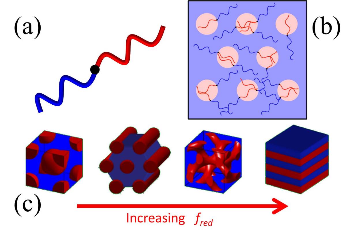
Block polymer overview
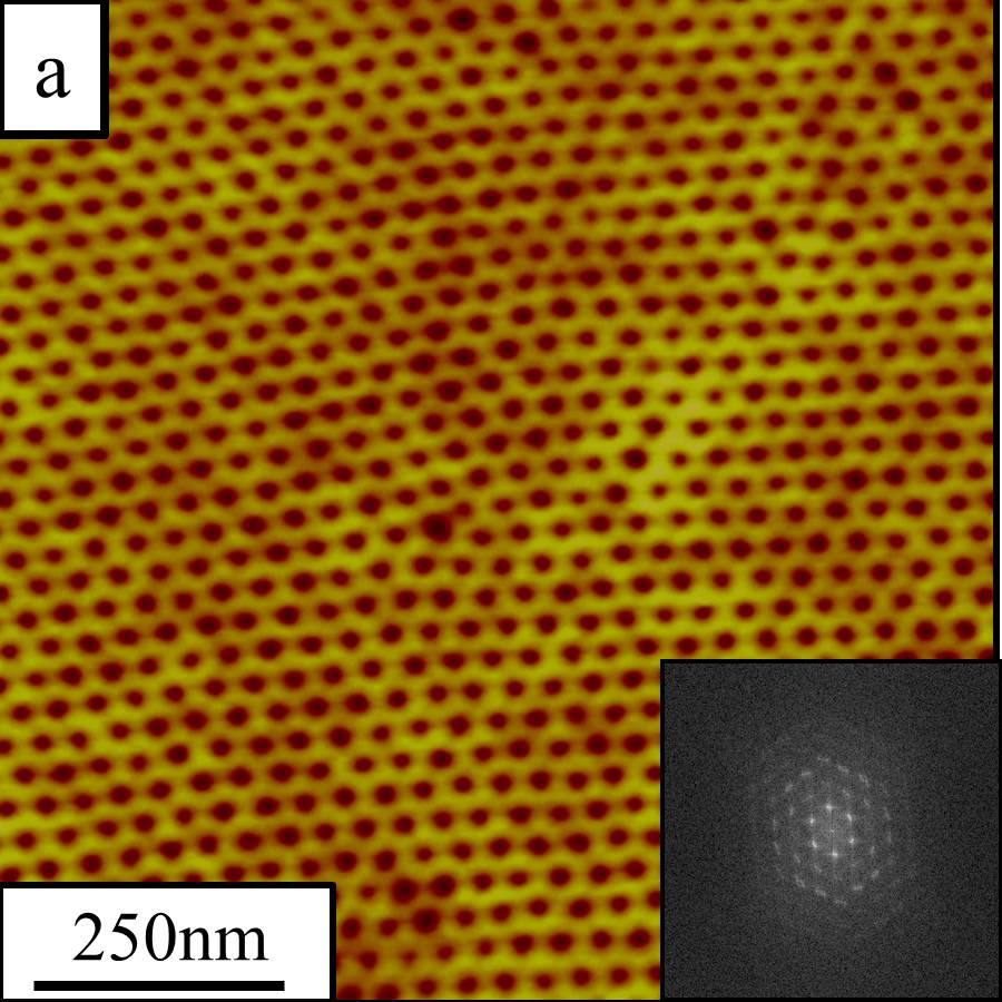
Directed self-assembly of a PS-PLA thin film |
The use of block polymers in nanolithography has emerged as a powerful technique for patterning large-area nanostructure arrays in a wide range of functional materials with a huge potential for expansion. Block polymers are comprised of two or more homopolymer subunits linked by a covalent bond. Their mutual immiscibility results in microphase separation leading to the formation of self-assembled periodic nanostructures in a variety of morphologies (holes, dots, lines and rings) with controllable size and density. Through the controlled introduction of organic solvent (a vapor that will solubilize the polymer blocks, increasing their mobility and decreasing their immiscibility), one can control the thermodynamics and kinetics of ordering as the solvent evaporates. Of critical importance, it is possible to direct the ordering of the phases during self-assembly, orient resultant features, and, speficially, produce hexagonally packed cylinders (critical to nanolithography) via this method. Upon successful solvent-induced ordering, the next logical step is transferring the well-organized pattern/template to a material of interest (e.g., magnetic, filtration, optoelectronic, biocompatible, etc.). This can be achieved by a variety of schemes, several of which we are working to develop in our lab. Specifically, we are looking at methods developed for magnetic materials. We have demonstrated unprecedented success in this regard, providing compatibility with many material classes. |
|
|
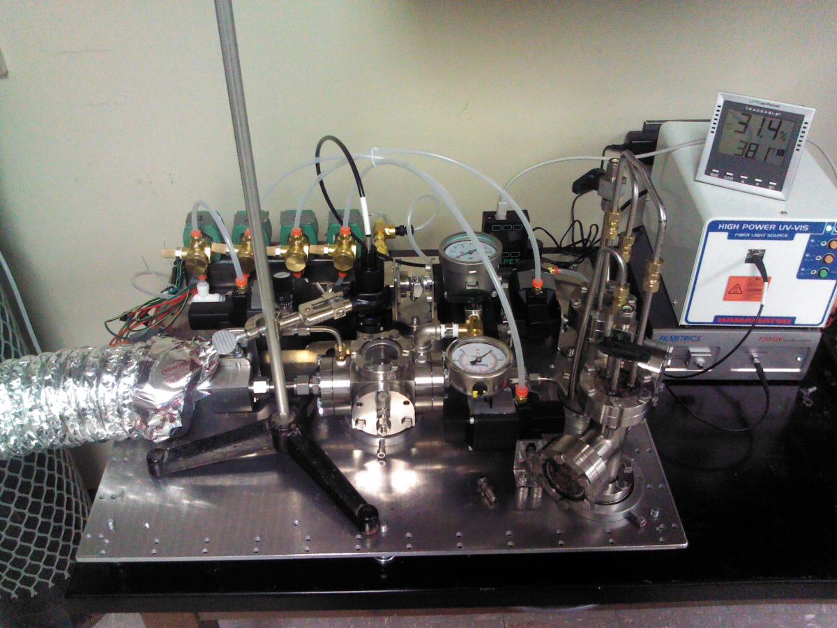
State-of-the-art Solvent Vapor Annealing Chamber... a labor of love with unprecedented control of all aspects of the solvent vapor annealing process, including swelling rate, concentration control, and solvent evaporation rate. For a 3-D Walkthough. Click Here |
|
Atomic Force Microscopy
|
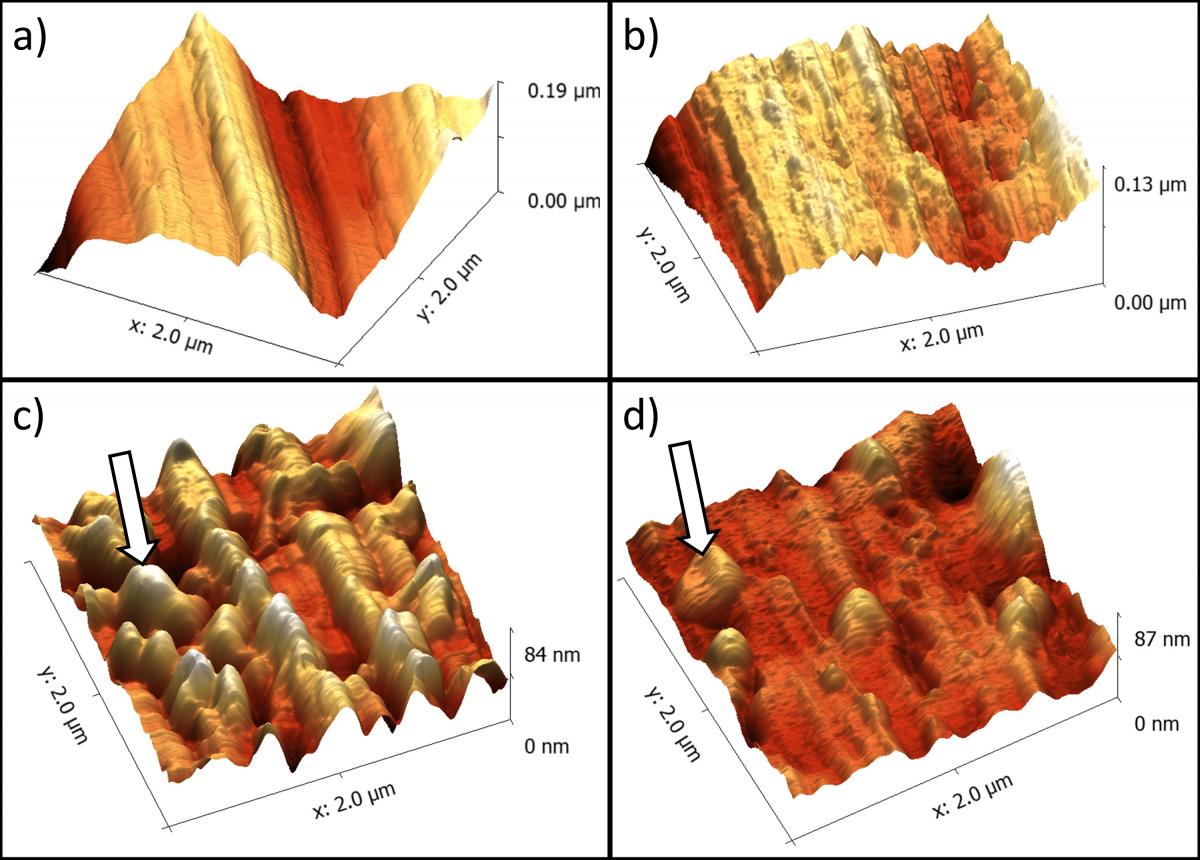
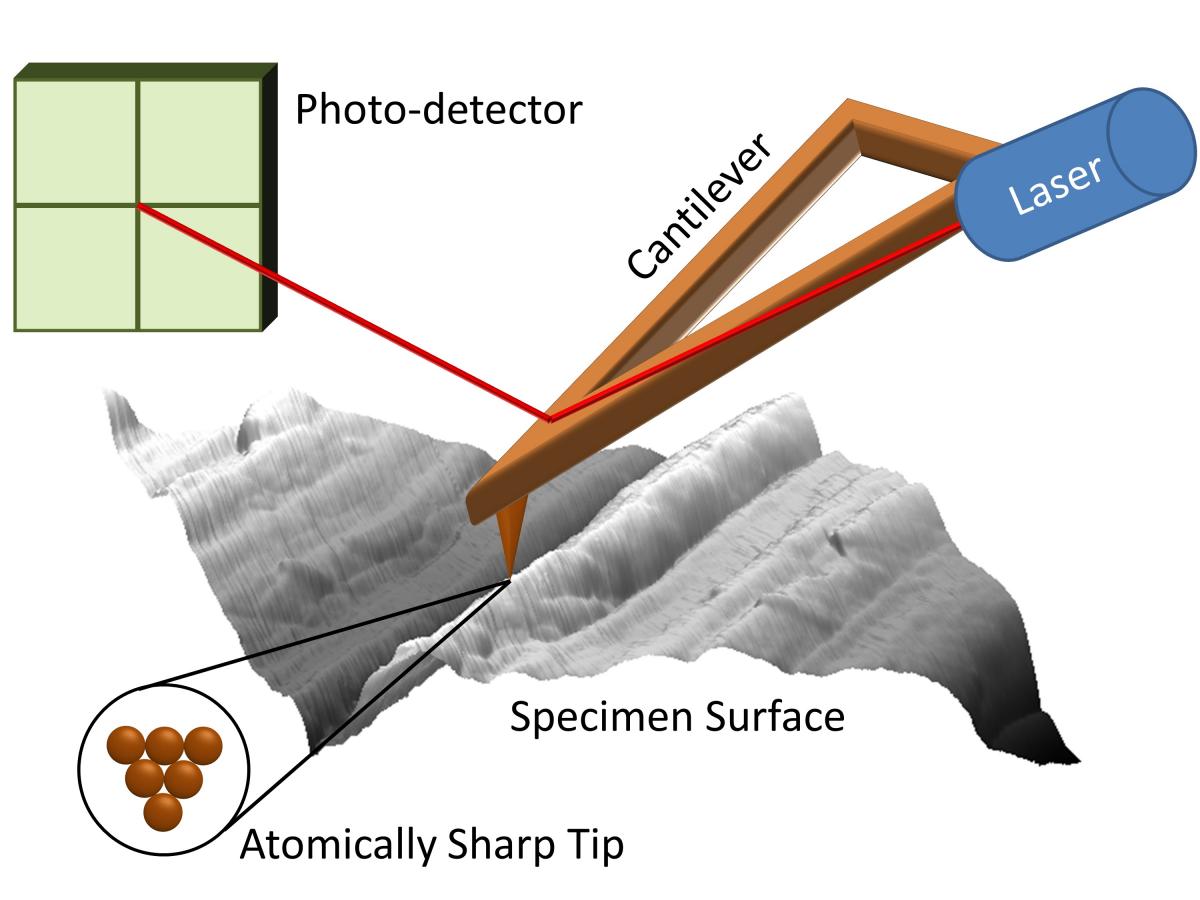
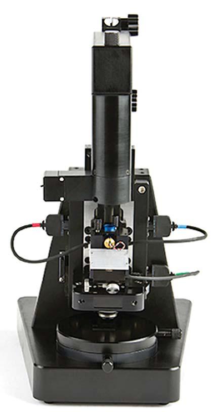
To study materials at the nanoscale, one must often be able to see at the nanoscale. We employ an Agilent 5420 Atomic Force Microscpe to view objects down to a resolution approaching 5 nm. We typically operate in both contact and tapping mode, dependent on material and feature size. This tool has been used to investigate the ordering properties of block polymer thin films, grain structure in sulfide-based opto-electronic thin films, as well as surface morphologies and cellular attachment of dental implant materials before and after cellular plating in verious states of wear. Presently, we are investigating methods for imaging in a liquid medium to allow for imaging of live cells and polymer films in various swollen states. |
|
|
Cellular features plated on substrates with varying roughness |
AFM Schmatic |
Agilent 5420 |
Magnetic Imaging
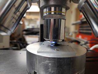
| Recently installed and commissioned MOKE Microscope and Magnetic Force Microscope | 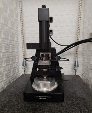 |
 |
Electronic Properties
|
|
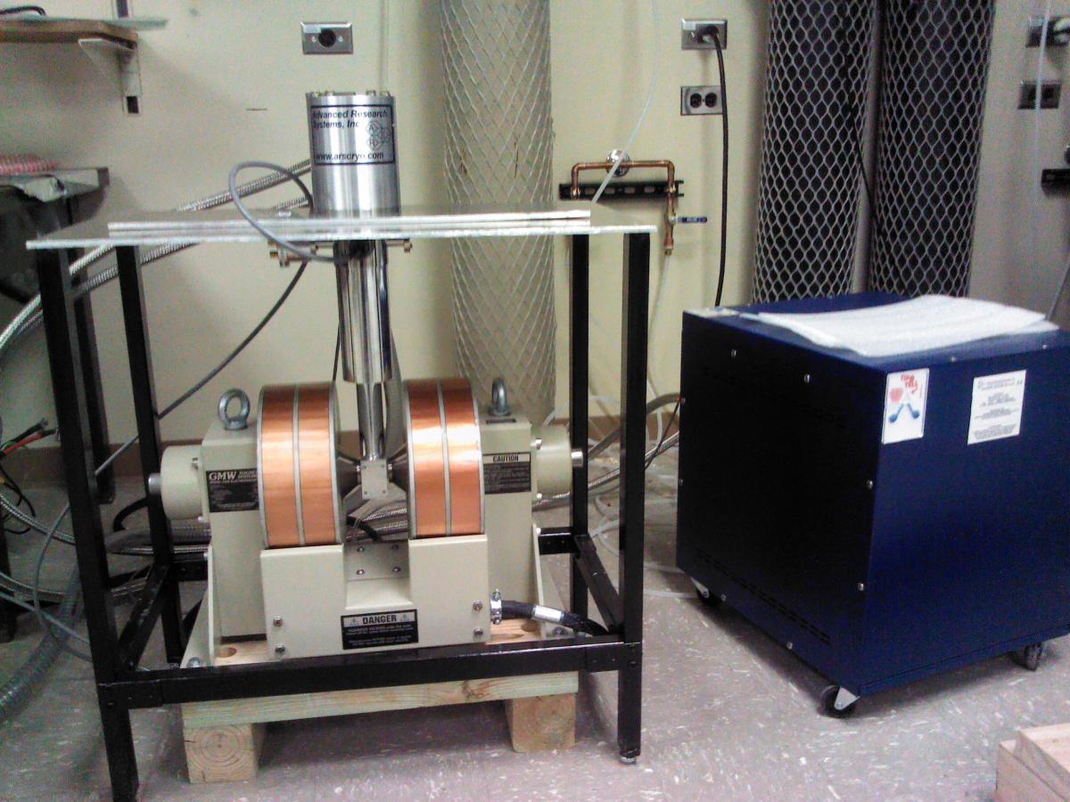
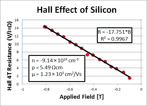
With the use of a 7K closed-cycle cryostat and a 1.6 T electromagnetic, we can perform:
This gives us the ability to reliably ascertain the electronc behavior, including charge carrier density and drift velocity.
|
Materials Deposition
|
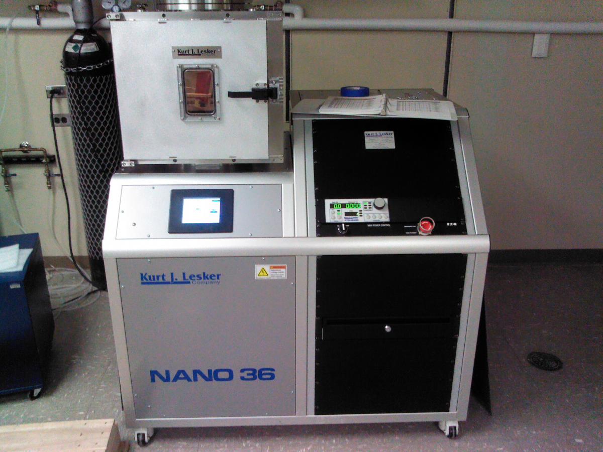
Thin film pre-cursor films are deposited via thermal evaporation in a Kurt J. Lesker NANO 36
|

